How to export Eagle PCB to gerber files
Eagle is a free EDA software ,there are a lot of engineers asked us how to export correct gerbers from Eagle. Here is a guide for you .
When you finished your design in Eagle, the last step before sending it off to the fab house is to generate gerber files. Autodesk EAGLE includes a handy computer-aided manufacturing (CAM) processor that allows you to load a CAM file and quickly generate the specific files you need for your design.
When you finished your design in Eagle, the last step before sending it off to the fab house is to generate gerber files. Autodesk EAGLE includes a handy computer-aided manufacturing (CAM) processor that allows you to load a CAM file and quickly generate the specific files you need for your design.
|
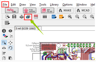
1. Open the CAM Processor
Open your PCB layout (.brd) file in Eagle, Click the “ CAM” button or choose “File -> CAM Processor”. This will open the CAM Processor tool that is used to generate the files. |
|
|
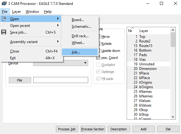
2. Select File -> Open -> Job
see the right side image. |
|
|
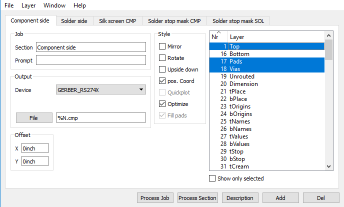
3. Then navigate to your default EAGLE cam folder, choose the gerb274x.cam file, select Open.
|
|
4. Adding a second silk screen (Optional)
If you look at the tabs, you will see that you don’t have a file for silk screen bottom. For simple boards, the silk screen is usually on the top layer so that you don’t need the bottom. But if you need silk screen on bottom layer as well, follow these steps:
Click “Add” -->Change Section to something like “Silk Screen SOL”-->Change File to “%N.pls”--->Deselect all layers-->Select layers 20 “Dimension”, 22 “bPlace” and 26 “bNames”
5. Select the Process Job button to create all of your Gerber files. You can find all of your generated Gerber files in the Autodesk EAGLE Control Panel in your project folder.
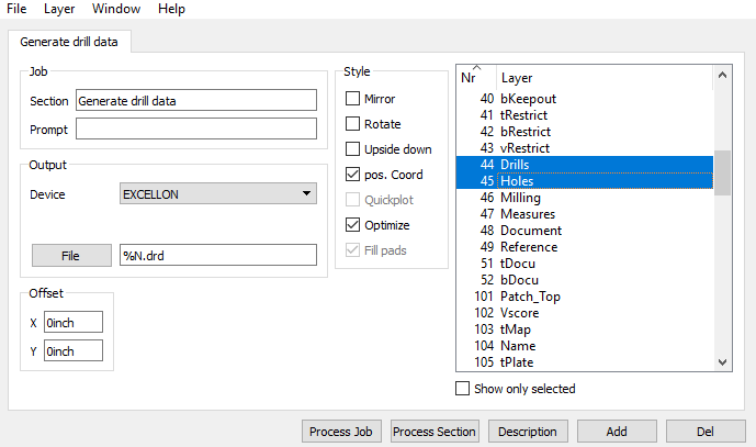
Generating Your Drill File1. Select the CAM Processor tool at the top of your interface or select File » CAM Processor to open the CAM processor dialog. 2. You now need to load a drill CAM job to get things started. Select File » Open » Job, and in your default EAGLE cam folder select the excellon.cam file, then select Open. 3. you'll now have a single Generate drill data tab available, which will grab the data from layers 44 Drills and 45 Holes, just what you need. Select the Process Job button to generate this file. |
|