• Home
  • About Us
    • Why Us
    • Our Team
    • Testimonials
  • PCB Fab
    • Standard PCB
    • ENEPIG PCB
    • HDI PCB
    • Large PCB
    • Impedance Control
    • Backdrilling PCB
    • Heavy Copper PCB
    • Via in Pad(POFV)
    • Quick Turn PCB
    • 10 layer PCB
    • High frequency PCB
    • MC/Aluminum PCB
    • Half hole plating
    • FPC Rigid-flex PCB
  • Service
    • PCB Assembly >
      • PCBA Products
      • PCBA Capability
    • Components Procuement
    • SMT Stencil
  • Technology
    • Optimize HDI
    • PCB Terminology
    • PCB Material
    • PCB panelization
    • PCB Stackup
    • Rigid-flex PCB design guidelines
    • Blind and burrid vias
    • Tip for PCB design
    • Generate gerber from Altium
    • Eagle PCB
    • KiCAD PCB
  • Contact
  • Blog
  • Products
Quick Turn PCB ENEPIG PCB 10 layer PCB Turnkey Assembly Rigid-flex PCB
  • Home
  • About Us
    • Why Us
    • Our Team
    • Testimonials
  • PCB Fab
    • Standard PCB
    • ENEPIG PCB
    • HDI PCB
    • Large PCB
    • Impedance Control
    • Backdrilling PCB
    • Heavy Copper PCB
    • Via in Pad(POFV)
    • Quick Turn PCB
    • 10 layer PCB
    • High frequency PCB
    • MC/Aluminum PCB
    • Half hole plating
    • FPC Rigid-flex PCB
  • Service
    • PCB Assembly >
      • PCBA Products
      • PCBA Capability
    • Components Procuement
    • SMT Stencil
  • Technology
    • Optimize HDI
    • PCB Terminology
    • PCB Material
    • PCB panelization
    • PCB Stackup
    • Rigid-flex PCB design guidelines
    • Blind and burrid vias
    • Tip for PCB design
    • Generate gerber from Altium
    • Eagle PCB
    • KiCAD PCB
  • Contact
  • Blog
  • Products

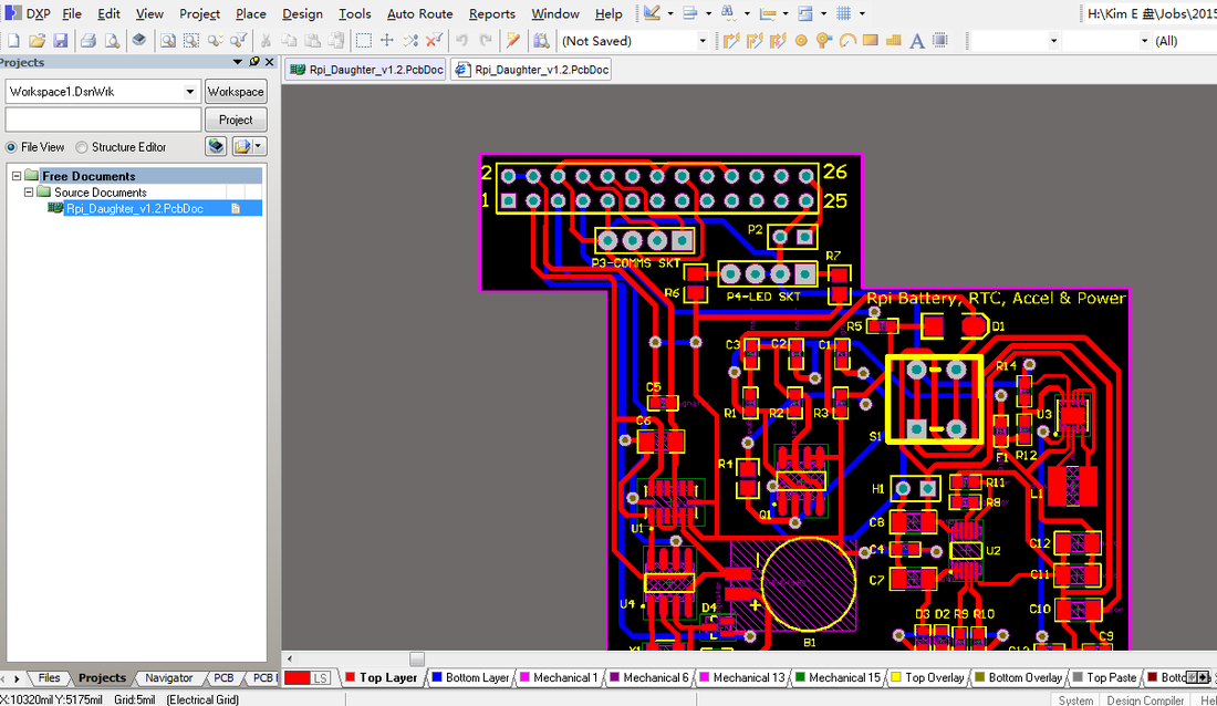
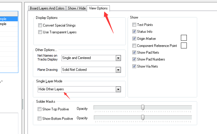
How to generate Gerber & Drill file from Altium

Gerber file is the Language of PCB Manufacturing.The Gerber file format, RS-274-D, for printed circuit board specification was originally introduced in 1980. Since, there have been two major revisions, X1 and X2. The currently used formats are open ASCII formats for 2-D binary images and serve as the unofficial industry standard for PCB design files. As most contract manufacturers (CMs) employ computer-aided manufacturing (CAM) equipment cable of reading Gerber files, their use provides you with the greatest pool of manufacturers capable of fabricating your boards.
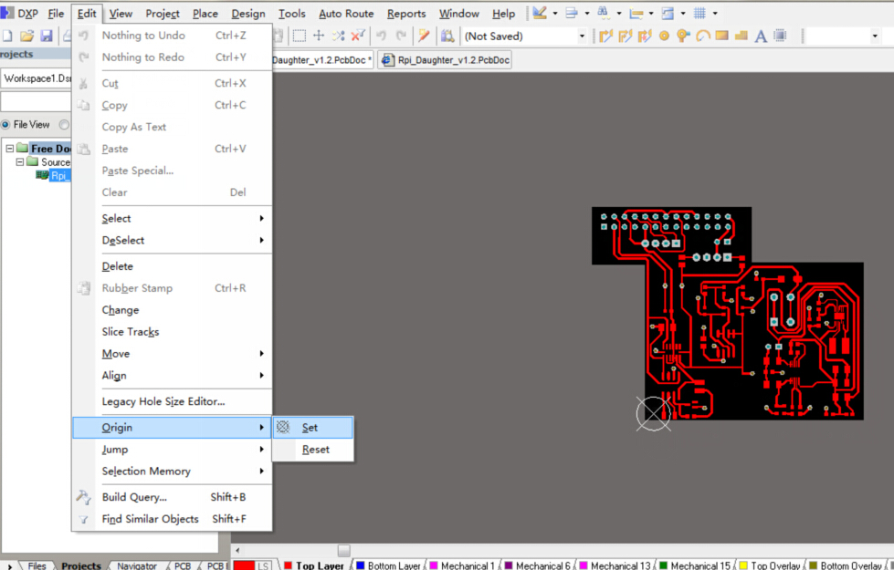
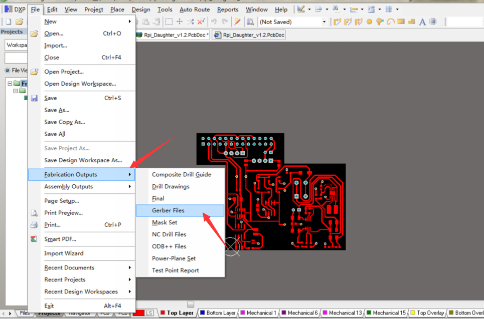
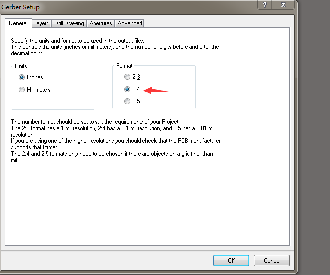
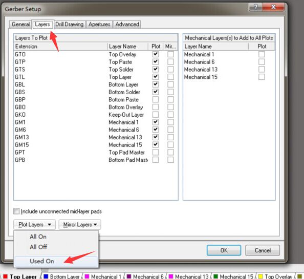
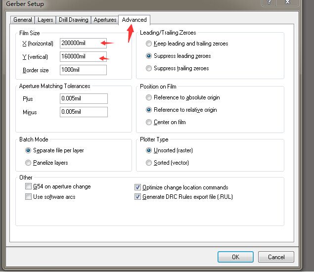
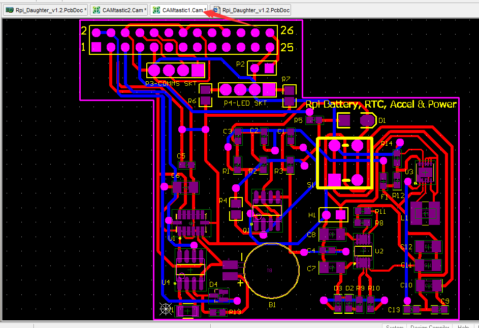
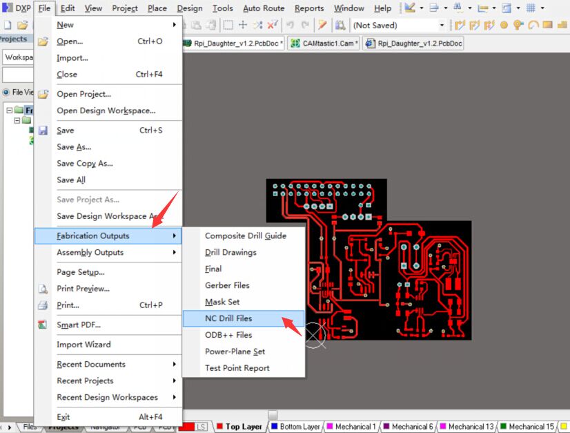
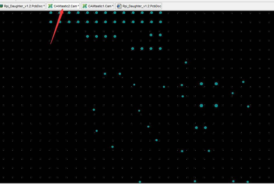
Many customers sent us wrong gerber file,even forgot drill file .For urgent jobs, the mistakes will waste much time .That is why we have to show how to generate correct gerber and drill file from Altium. There are any versions for Altium,we can not keep update,here is an example for Altium 6.9. New versions will be similar.

1, this is what we see when open your design file . For PCB manufacturing,PCBDOC is the only and right file for us.
图片
2,before generate,check each layer is correct.Please do not forget the outline layer. L--->view options-->Hide other layers
图片
3,All layer is correct,then set original datum.
 Edit--->Origin--->Set. Many customers did not set origin,that makes each gerber layers are in different positions.
图片
4,Export gerber file now. File-->Fabrication outputs-->Gerber files.
图片
Gerber format setting. 2:4 is preferred for all.
图片
Click layers-->Used on.you will see your defined layers.
图片
Some boards are very large ,or some features are far away from your board.so change the film size. then Click OK ,gerber files are in the same path with the design now.
图片
When gerber file generated correctly,it looks like below.
图片
5, Generate Drill file.File-->Fabrication outputs-->NC drill, drill format,2:3 or 2:4 is OK for us .
图片
When drill file generated correctly,it looks like below.
图片
Get an Instant PCB Quote Now
Download

Mullilayer standard stack up
PCB Fab check list 
PCB capability
Sample BOM
Flex PCB material
High frequency material
Generate gerber
FPC design guide
IC,LPC178,original&new
Original&New LPC178 chips
Our PCBs

Flex PCB
Rigid-flex PCB
RF board
Heavy copper PCB
20 layer PCB
10 layer PCB
HDI PCB
ENEPIG PCB
Control impedance
Quick Turn boards

turnkey assembly service
Turnkey assembly service
Additional Products&Service
Components Sourcing
PCB Assemble
SMT Stencil
Cable assemble
About Us
Why Us
WorkShop
Tips for PCB design
Testimonials
​Contact Us
Technology
Backdrilling PCB
Generate Gerber
Rigid-Flex Design Guide
10 Layer PCB
Impedance control
Heavy Copper PCB
​
PCB Assembly
Quick Turn Circuits
HDI boards
Rigid-Flex circuits
RF/Microwave/HF PCB
MC PCB/Al-substrate
ENEPIG PCB
​Components procument


order online
Payment
Shipment
FAQ
SMT stencil
Via in Pad (POFV)
0.38mm pitch CSP

Download
PCB Capability
Sample BOM
PCB check list
Multilayer stack up
​Stencils
PCB material

​
All rights reserved,2007-2022 Storm Circuit Technology  Ltd  
Blog: www.stormcircuit.net
Picture
storm pcb: www.stormpcb.com
Picture
Picture
Made with love  by Storm Circuit in China

Picture
Picture

    news and discount

Subscribe
  • Home
  • About Us
    • Why Us
    • Our Team
    • Testimonials
  • PCB Fab
    • Standard PCB
    • ENEPIG PCB
    • HDI PCB
    • Large PCB
    • Impedance Control
    • Backdrilling PCB
    • Heavy Copper PCB
    • Via in Pad(POFV)
    • Quick Turn PCB
    • 10 layer PCB
    • High frequency PCB
    • MC/Aluminum PCB
    • Half hole plating
    • FPC Rigid-flex PCB
  • Service
    • PCB Assembly >
      • PCBA Products
      • PCBA Capability
    • Components Procuement
    • SMT Stencil
  • Technology
    • Optimize HDI
    • PCB Terminology
    • PCB Material
    • PCB panelization
    • PCB Stackup
    • Rigid-flex PCB design guidelines
    • Blind and burrid vias
    • Tip for PCB design
    • Generate gerber from Altium
    • Eagle PCB
    • KiCAD PCB
  • Contact
  • Blog
  • Products