• Home
  • About Us
    • Why Us
    • Our Team
    • Testimonials
  • PCB Fab
    • Standard PCB
    • ENEPIG PCB
    • HDI PCB
    • Large PCB
    • Impedance Control
    • Backdrilling PCB
    • Heavy Copper PCB
    • Via in Pad(POFV)
    • Quick Turn PCB
    • 10 layer PCB
    • High frequency PCB
    • MC/Aluminum PCB
    • Half hole plating
    • FPC Rigid-flex PCB
  • Service
    • PCB Assembly >
      • PCBA Products
      • PCBA Capability
    • Components Procuement
    • SMT Stencil
  • Technology
    • Optimize HDI
    • PCB Terminology
    • PCB Material
    • PCB panelization
    • PCB Stackup
    • Rigid-flex PCB design guidelines
    • Blind and burrid vias
    • Tip for PCB design
    • Generate gerber from Altium
    • Eagle PCB
    • KiCAD PCB
  • Contact
  • Blog
  • Products
Quick Turn PCB ENEPIG PCB 10 layer PCB Turnkey Assembly Rigid-flex PCB
  • Home
  • About Us
    • Why Us
    • Our Team
    • Testimonials
  • PCB Fab
    • Standard PCB
    • ENEPIG PCB
    • HDI PCB
    • Large PCB
    • Impedance Control
    • Backdrilling PCB
    • Heavy Copper PCB
    • Via in Pad(POFV)
    • Quick Turn PCB
    • 10 layer PCB
    • High frequency PCB
    • MC/Aluminum PCB
    • Half hole plating
    • FPC Rigid-flex PCB
  • Service
    • PCB Assembly >
      • PCBA Products
      • PCBA Capability
    • Components Procuement
    • SMT Stencil
  • Technology
    • Optimize HDI
    • PCB Terminology
    • PCB Material
    • PCB panelization
    • PCB Stackup
    • Rigid-flex PCB design guidelines
    • Blind and burrid vias
    • Tip for PCB design
    • Generate gerber from Altium
    • Eagle PCB
    • KiCAD PCB
  • Contact
  • Blog
  • Products

How to save cost and make easily for your HDI PCB?


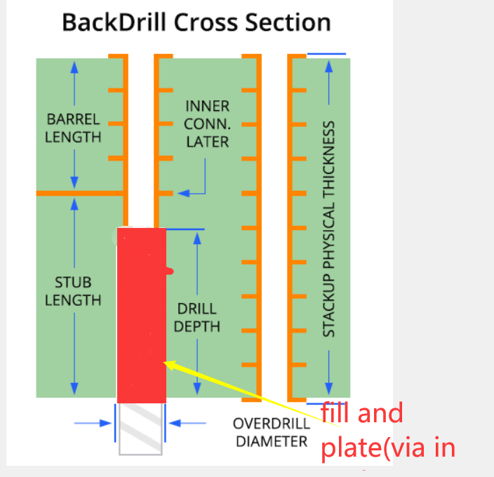
​We have many customers sent us HDI PCB file ,but the files are very complex and high cost 
to do .some PCB designers do not have much experience in the PCB manufaturing,some files 
are unable to do .We--Storm Circuit has over 15 years experience in PCB fabrication and assembly.
Our engineers have enough experience to optimize your HDI PCB.

Here is an example. This is a 6 layer PCB ,Rogers 4003,Blind vias ( 0.25mm)from L1-L2,L1-L3,L1-L4,
thickness is 1.6mm.
So,how to do ?The key issue for PCB manufacturer is the blind vias. L1-L2 and L1-L4 is OK,no problem to do ,
The board must be done like an 8 layer with three cores (L1/L2,L3/L4,L5/L6).The stackup must be done with laser drilling for L1-L2
L1-L3,L1-L4. So blind vias will be changed from 0.25mm to 0.1mm. Customer does not agree.

 OK, then the next problem is drill 1-3 is too difficult for Rogers material ,
even many PCB factories can not make Rogers material with blind/buried vias. Rogers material 
is different as FR4 material. This design must be Rogers material ,it is a high frequency application.

FR4 material is unacceptable to do ,and laser drilling is unacceptable too.
There is another way?
Our senior PCB engineer Kim Chan who has over 17 years experience in PCB manufacturing
adviced to use back-drill and via in pad technology.
That is 1-2 is a core, drill as usual , and 1-3 1-4 will be drilled as through holes first.Then, in the last 
process, we will drill out the copper for 3-6 /4-6,this is back-drill.But we will see holes at bottom side,
it is different with the customer's design. Then ,we will fill and plate the back drill holes,so nothing we can see.
This processs cost is a bit lower than FR4 with 1-2 1-3 1-4, and easy to do . Any layer HDI prototypes will be at least US$2000,but we used back drill and via in pad,cost cut down more than 30%.
Of course, we confirmed with customer and get his approval to proceed. 
Rogers material with blind/buried vias ,we can do!
If you have any HDI inquiries, please email to us directly.
We can make any layer HDI for 14 Layers,like below structure .
Our any layer HDI partner is Foxconn,one of the top PCB manufacturers in the world.
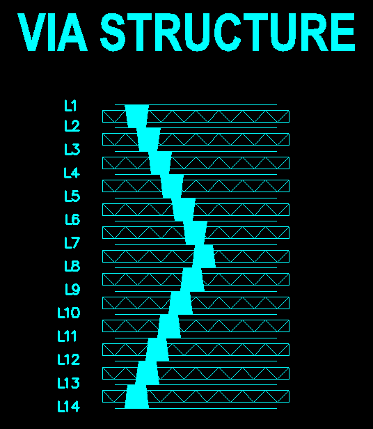
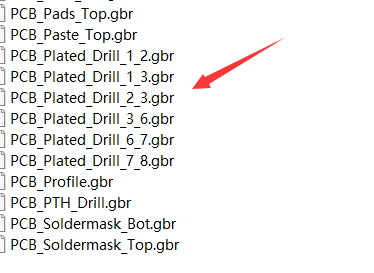
Picture
Picture
Picture
Picture
Picture
8 Layer HDI,
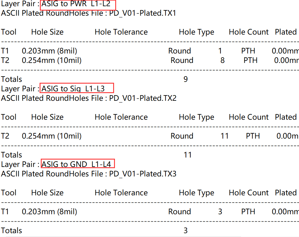
drill 1-2
drill 2-3
drill 3-6
drill 6-7
​drill 7-8
min via 0.1mm, min trace/space 0.076/0.076mm
Storm Circuit offer quick turn HDI PCB from 5 days to 20 days.  the above 8 layer HDI ,we sent out in 6 days with quick turn service. 

About Us
Why Us
WorkShop
Tips for PCB design
Testimonials
​Contact Us
Technology
Backdrilling PCB
Generate Gerber
Rigid-Flex Design Guide
10 Layer PCB
Impedance control
Heavy Copper PCB
​
PCB Assembly
Quick Turn Circuits
HDI boards
Rigid-Flex circuits
RF/Microwave/HF PCB
MC PCB/Al-substrate
ENEPIG PCB
​Components procument


order online
Payment
Shipment
FAQ
SMT stencil
Via in Pad (POFV)
0.38mm pitch CSP

Download
PCB Capability
Sample BOM
PCB check list
Multilayer stack up
​Stencils
PCB material

​
All rights reserved,2007-2022 Storm Circuit Technology  Ltd  
Blog: www.stormcircuit.net
Picture
storm pcb: www.stormpcb.com
Picture
Picture
Made with love  by Storm Circuit in China

Picture
Picture

    news and discount

Subscribe
  • Home
  • About Us
    • Why Us
    • Our Team
    • Testimonials
  • PCB Fab
    • Standard PCB
    • ENEPIG PCB
    • HDI PCB
    • Large PCB
    • Impedance Control
    • Backdrilling PCB
    • Heavy Copper PCB
    • Via in Pad(POFV)
    • Quick Turn PCB
    • 10 layer PCB
    • High frequency PCB
    • MC/Aluminum PCB
    • Half hole plating
    • FPC Rigid-flex PCB
  • Service
    • PCB Assembly >
      • PCBA Products
      • PCBA Capability
    • Components Procuement
    • SMT Stencil
  • Technology
    • Optimize HDI
    • PCB Terminology
    • PCB Material
    • PCB panelization
    • PCB Stackup
    • Rigid-flex PCB design guidelines
    • Blind and burrid vias
    • Tip for PCB design
    • Generate gerber from Altium
    • Eagle PCB
    • KiCAD PCB
  • Contact
  • Blog
  • Products