HDI-HIGH DENSITY INTERCONNECT PCB
|

|
HDI,1+N+1, Standard and quick turn lead time for prototypes. (<1 sq meter).
2+N+2 ,3+N+3. PCB gerber file is required to get correct cost and lead time |
|
Any layer/ELIC (every layer interconnection) is the most complex PCB to do.We made a few of such prototype PCBs.
|
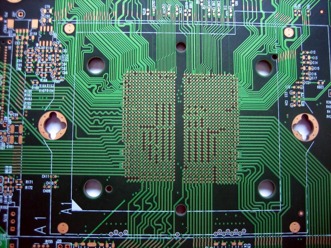
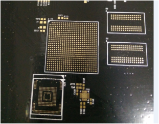
10 Layer HDI board,0.5mm pitch BGA. 4/4mil,0.15mm vias,Tablet PC mother board

|
8 layer HDI board ,impedence control,3/3mil 0.1mm vias,Telecom board,burried/blind vias with 0.1mm
|
|
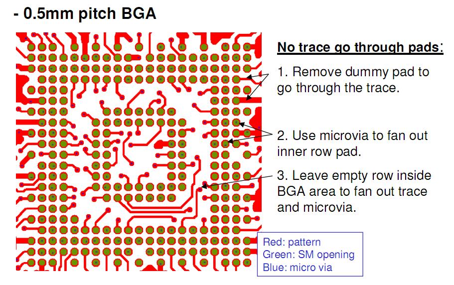
0.5mm pitch BGA design guide--NO trace go through BGA pads
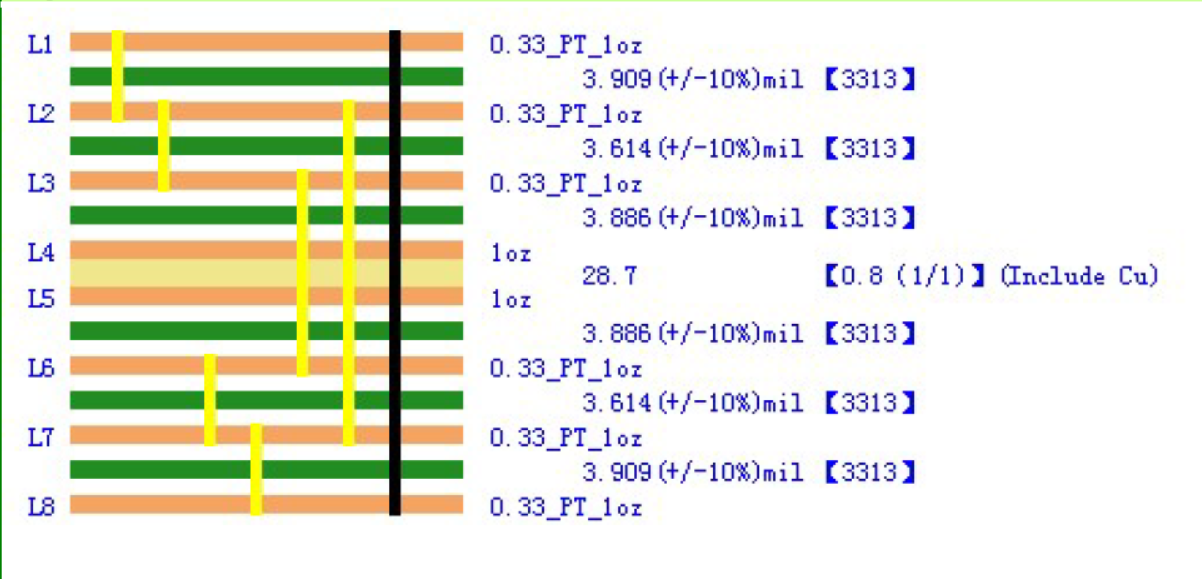
Gerber file for 6 layer HDI board.
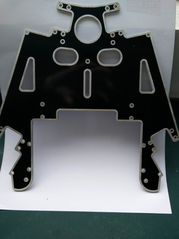
Specification:FR4,TG170,1.2mm,1oz for all layers. min via:0.15mm, min trace/space:0.1/0.1mm. Impedance control,Black solder mask,ENIG Blind/burried vias (L1-L2,L1-L3,L4-L6,L5-L6) 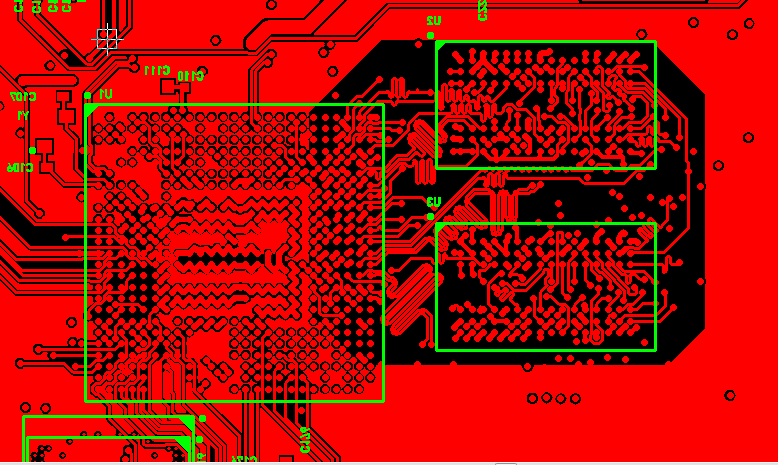
|
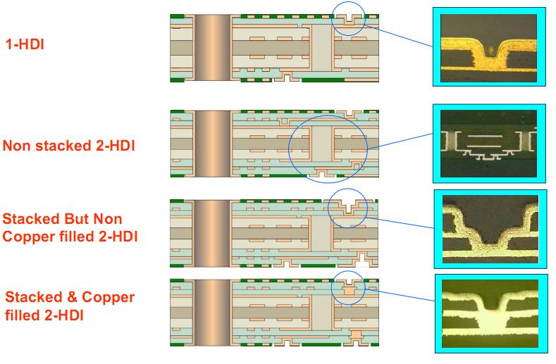
Examples of HDI stack up
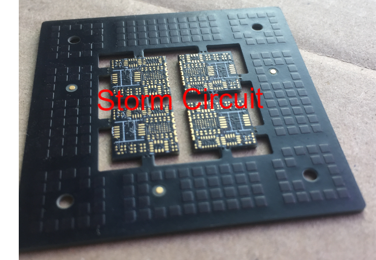
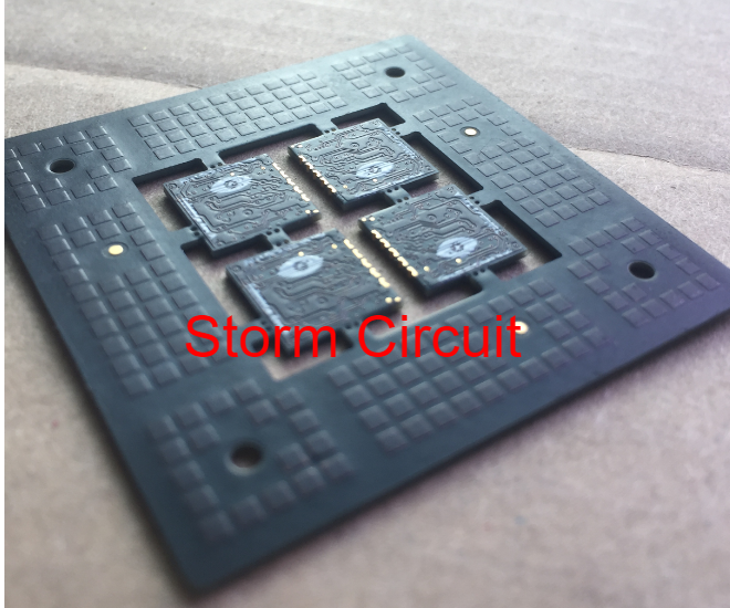
Real Board for the left Gerber.
|
Download
Multilayer standard stack up
PCB Fab check list
PCB capability
Sample BOM
Flex PCB material
High frequency material
Multilayer standard stack up
PCB Fab check list
PCB capability
Sample BOM
Flex PCB material
High frequency material
Immersion Silver ,2.4mm
Our PCBs
Flex PCB
Rigid-flex PCB
RF board
Heavy copper PCB
20 layer PCB
10 layer PCB
HDI PCB
ENEPIG PCB
Control impedance
Quick Turn boards
MC PCB
Flex PCB
Rigid-flex PCB
RF board
Heavy copper PCB
20 layer PCB
10 layer PCB
HDI PCB
ENEPIG PCB
Control impedance
Quick Turn boards
MC PCB
4 layer rigid-flex board