• Home
  • About Us
    • Why Us
    • Our Team
    • Testimonials
  • PCB Fab
    • Standard PCB
    • ENEPIG PCB
    • HDI PCB
    • Large PCB
    • Impedance Control
    • Backdrilling PCB
    • Heavy Copper PCB
    • Via in Pad(POFV)
    • Quick Turn PCB
    • 10 layer PCB
    • High frequency PCB
    • MC/Aluminum PCB
    • Half hole plating
    • FPC Rigid-flex PCB
  • Service
    • PCB Assembly >
      • PCBA Products
      • PCBA Capability
    • Components Procuement
    • SMT Stencil
  • Technology
    • Optimize HDI
    • PCB Terminology
    • PCB Material
    • PCB panelization
    • PCB Stackup
    • Rigid-flex PCB design guidelines
    • Blind and burrid vias
    • Tip for PCB design
    • Generate gerber from Altium
    • Eagle PCB
    • KiCAD PCB
  • Contact
  • Blog
  • Products
Quick Turn PCB ENEPIG PCB 10 layer PCB Turnkey Assembly Rigid-flex PCB
  • Home
  • About Us
    • Why Us
    • Our Team
    • Testimonials
  • PCB Fab
    • Standard PCB
    • ENEPIG PCB
    • HDI PCB
    • Large PCB
    • Impedance Control
    • Backdrilling PCB
    • Heavy Copper PCB
    • Via in Pad(POFV)
    • Quick Turn PCB
    • 10 layer PCB
    • High frequency PCB
    • MC/Aluminum PCB
    • Half hole plating
    • FPC Rigid-flex PCB
  • Service
    • PCB Assembly >
      • PCBA Products
      • PCBA Capability
    • Components Procuement
    • SMT Stencil
  • Technology
    • Optimize HDI
    • PCB Terminology
    • PCB Material
    • PCB panelization
    • PCB Stackup
    • Rigid-flex PCB design guidelines
    • Blind and burrid vias
    • Tip for PCB design
    • Generate gerber from Altium
    • Eagle PCB
    • KiCAD PCB
  • Contact
  • Blog
  • Products

Quick Turn Circuits

Some customers asked us how quickly we can do for PCB and PCB Assembly.Here,you will get the right answer.
You can get 1-2 layer PCBs  in 48 hours, and 4-6 layer  2-3 working days,8 layer 3-4 working days. All quick turn boards are also with top quality . We even did 16 layer PCB within 12 days. 

Submit your PCB specifications by emailing us your Gerber Files or by filling out the online PCB Quote form. There, you will attach your gerber files or design files and send via form to us .we are confident that we will be able to help you with your project.

Get Your PCBs in 2 Days Now
You can find our standard lead time and quick turn lead time as below. Once you try us,you will know how quickly we offer. 
Layers Standard Lead Time Fast Turn Around Lead Time
1 Layer 4 working days 1-2 days
2 Layer 5 working days 1-2 days
4 layer 6 working days 2-3 days
6 Layer 6 working days 2-3 days
8 Layer 8 working days 3-4 days
4 Layer PCB witH gold fingers,thickness 0.8mm. fastest service 4 days including shipping time (2 days).
quick turn for 4 layer gold fingers PCB
Quick turn USB project in 2 weeks.including PCB manufacturing,components sourcing and assemble.
Quick turn for USB project in 2 weeks
Quick Turn 4 layer with Rogers 4003C PCB manufacturing and assembly in 2 weeks.
Rogers 4003C assembly
Quick Turn for MC PCB with Bergquist ,Matt Black solder mask 1.5mm in 1 week.
bergquist MC PCB
Download

Mullilayer standard stack up
PCB Fab check list 
PCB capability
Sample BOM
Flex PCB material
High frequency material
8 HDI board with impedance control
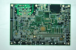
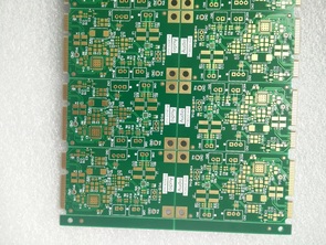
8 layer with impedance control
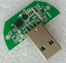
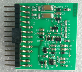
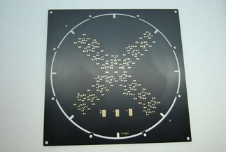
Our PCBs

Flex PCB
Rigid-flex PCB
RF board
Heavy copper PCB
20 layer PCB
10 layer PCB
HDI PCB
ENEPIG PCB
Control impadence
Quick Turn boards
MC PCB
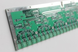
6 layer with control depth slots
Additional Products&Service

Components Sourcing
PCB Assemble
SMT Stencil
Cable assemble


About Us
Why Us
WorkShop
Tips for PCB design
Testimonials
​Contact Us
Technology
Backdrilling PCB
Generate Gerber
Rigid-Flex Design Guide
10 Layer PCB
Impedance control
Heavy Copper PCB
​
PCB Assembly
Quick Turn Circuits
HDI boards
Rigid-Flex circuits
RF/Microwave/HF PCB
MC PCB/Al-substrate
ENEPIG PCB
​Components procument


order online
Payment
Shipment
FAQ
SMT stencil
Via in Pad (POFV)
0.38mm pitch CSP

Download
PCB Capability
Sample BOM
PCB check list
Multilayer stack up
​Stencils
PCB material

​
All rights reserved,2007-2022 Storm Circuit Technology  Ltd  
Blog: www.stormcircuit.net
Picture
storm pcb: www.stormpcb.com
Picture
Picture
Made with love  by Storm Circuit in China

Picture
Picture

    news and discount

Subscribe
  • Home
  • About Us
    • Why Us
    • Our Team
    • Testimonials
  • PCB Fab
    • Standard PCB
    • ENEPIG PCB
    • HDI PCB
    • Large PCB
    • Impedance Control
    • Backdrilling PCB
    • Heavy Copper PCB
    • Via in Pad(POFV)
    • Quick Turn PCB
    • 10 layer PCB
    • High frequency PCB
    • MC/Aluminum PCB
    • Half hole plating
    • FPC Rigid-flex PCB
  • Service
    • PCB Assembly >
      • PCBA Products
      • PCBA Capability
    • Components Procuement
    • SMT Stencil
  • Technology
    • Optimize HDI
    • PCB Terminology
    • PCB Material
    • PCB panelization
    • PCB Stackup
    • Rigid-flex PCB design guidelines
    • Blind and burrid vias
    • Tip for PCB design
    • Generate gerber from Altium
    • Eagle PCB
    • KiCAD PCB
  • Contact
  • Blog
  • Products