• Home
  • About Us
    • Why Us
    • Our Team
    • Testimonials
  • PCB Fab
    • Standard PCB
    • ENEPIG PCB
    • HDI PCB
    • Large PCB
    • Impedance Control
    • Backdrilling PCB
    • Heavy Copper PCB
    • Via in Pad(POFV)
    • Quick Turn PCB
    • 10 layer PCB
    • High frequency PCB
    • MC/Aluminum PCB
    • Half hole plating
    • FPC Rigid-flex PCB
  • Service
    • PCB Assembly >
      • PCBA Products
      • PCBA Capability
    • Components Procuement
    • SMT Stencil
  • Technology
    • Optimize HDI
    • PCB Terminology
    • PCB Material
    • PCB panelization
    • PCB Stackup
    • Rigid-flex PCB design guidelines
    • Blind and burrid vias
    • Tip for PCB design
    • Generate gerber from Altium
    • Eagle PCB
    • KiCAD PCB
  • Contact
  • Blog
  • Products
Quick Turn PCB ENEPIG PCB 10 layer PCB Turnkey Assembly Rigid-flex PCB
  • Home
  • About Us
    • Why Us
    • Our Team
    • Testimonials
  • PCB Fab
    • Standard PCB
    • ENEPIG PCB
    • HDI PCB
    • Large PCB
    • Impedance Control
    • Backdrilling PCB
    • Heavy Copper PCB
    • Via in Pad(POFV)
    • Quick Turn PCB
    • 10 layer PCB
    • High frequency PCB
    • MC/Aluminum PCB
    • Half hole plating
    • FPC Rigid-flex PCB
  • Service
    • PCB Assembly >
      • PCBA Products
      • PCBA Capability
    • Components Procuement
    • SMT Stencil
  • Technology
    • Optimize HDI
    • PCB Terminology
    • PCB Material
    • PCB panelization
    • PCB Stackup
    • Rigid-flex PCB design guidelines
    • Blind and burrid vias
    • Tip for PCB design
    • Generate gerber from Altium
    • Eagle PCB
    • KiCAD PCB
  • Contact
  • Blog
  • Products

What is PCB?

Storm Circuit business cardFree Gift--Storm Circuit Ruler
PCB is the short name of Printed Circuit Boards.however ,some ones also call it as PWB--Printed Wire boards.There are many different types of boards,such as rigid PCB--this is what we often say and used in the world. Flexible PCB--FPC,it used to connect two or more parts,see your camera or mobile ,FPC connects LCD to mother board. Rigid-flex board--a board with some part are flex and others are rigid.
Most are multi-layers board.Aluminum board---the base material is aluminum ,most used in LED,it requires high thermal conductivity. 

PCB manufacturing process is  very complex ,there are over 30 steps ,we will show you a very
​simple process here.

Double sided PCB:
Cutting Material-->Drilling holes--->Plating holes--->Outer layer
-->Etching-->Solder mask-->Silkscreen-->HAL(Gold)-->CNC (routing,v-cut)-->Testing-->Final inspection


Multilayer PCB:
Cutting Material-->Inner layer-->Press (stackup)--->Drilling holes
​-->Plating--->Outer layer -->Etching-->Solder mask-->Silkscreen
--->HAL(Gold)-->CNC (routing,v-cut)-->Testing-->Final inspection

Quote Now

Quick Turn Circuit Boards

We offer the best quick turn boards with very competitive price for prototypes to volume in 1-10 days.Click here to see details.
Layers Standard L/T Express L/T
1 Layer 4 working days 1-2 days
2 Layer 5 working days 1-2 days
4 layer 6 working days 2-3 days
6 Layer 6 working days 2-3 days
8 Layer 8 working days 3-4 days

High Technology Boards

We offer many hi-tech boards with 3/3 mil ,0.1mm vias,6-30 layers,impedence control,countersink holes,HDI.rigid-flex boards
8 layer quick turn PCB
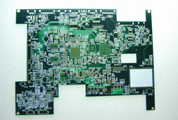
8 Layer quick turn board

PCB Manufacturing Process

Some customers do not know what process we have made in PCB.Here we will show you how to make step by step.
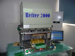
PCB fixture testing machine
PCB fixture tester

High Frequency PCB

High frequency board (RF board or microwave board) used in many fields.We have all kinds of material for you,eg,Rogers,Taconic, Arlon,PTFE.
Taconic TL32 ,high frequency boards
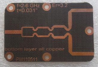
Taconic TL32 ,RF Circuits
HDI,1+N+1, Standard and quick turn lead time for prototypes. (<1 sq meter).
2+N+2 ,3+N+3. PCB gerber file is required to get correct cost and lead time.
HDI 1+N+1 Quick Turn Lead time Standard Lead time
4 layer 5 working days 8 working days
6 layer 6 working days 9 working days
8 layer 7 working days 11 working days
10 layer 8 working days 12 working days
About Us
Why Us
WorkShop
Tips for PCB design
Testimonials
​Contact Us
Technology
Backdrilling PCB
Generate Gerber
Rigid-Flex Design Guide
10 Layer PCB
Impedance control
Heavy Copper PCB
​
PCB Assembly
Quick Turn Circuits
HDI boards
Rigid-Flex circuits
RF/Microwave/HF PCB
MC PCB/Al-substrate
ENEPIG PCB
​Components procument


order online
Payment
Shipment
FAQ
SMT stencil
Via in Pad (POFV)
0.38mm pitch CSP

Download
PCB Capability
Sample BOM
PCB check list
Multilayer stack up
​Stencils
PCB material

​
All rights reserved,2007-2022 Storm Circuit Technology  Ltd  
Blog: www.stormcircuit.net
Picture
storm pcb: www.stormpcb.com
Picture
Picture
Made with love  by Storm Circuit in China

Picture
Picture

    news and discount

Subscribe
  • Home
  • About Us
    • Why Us
    • Our Team
    • Testimonials
  • PCB Fab
    • Standard PCB
    • ENEPIG PCB
    • HDI PCB
    • Large PCB
    • Impedance Control
    • Backdrilling PCB
    • Heavy Copper PCB
    • Via in Pad(POFV)
    • Quick Turn PCB
    • 10 layer PCB
    • High frequency PCB
    • MC/Aluminum PCB
    • Half hole plating
    • FPC Rigid-flex PCB
  • Service
    • PCB Assembly >
      • PCBA Products
      • PCBA Capability
    • Components Procuement
    • SMT Stencil
  • Technology
    • Optimize HDI
    • PCB Terminology
    • PCB Material
    • PCB panelization
    • PCB Stackup
    • Rigid-flex PCB design guidelines
    • Blind and burrid vias
    • Tip for PCB design
    • Generate gerber from Altium
    • Eagle PCB
    • KiCAD PCB
  • Contact
  • Blog
  • Products