• Home
  • About Us
    • Why Us
    • Our Team
    • Testimonials
  • PCB Fab
    • Standard PCB
    • ENEPIG PCB
    • HDI PCB
    • Large PCB
    • Impedance Control
    • Backdrilling PCB
    • Heavy Copper PCB
    • Via in Pad(POFV)
    • Quick Turn PCB
    • 10 layer PCB
    • High frequency PCB
    • MC/Aluminum PCB
    • Half hole plating
    • FPC Rigid-flex PCB
  • Service
    • PCB Assembly >
      • PCBA Products
      • PCBA Capability
    • Components Procuement
    • SMT Stencil
  • Technology
    • Optimize HDI
    • PCB Terminology
    • PCB Material
    • PCB panelization
    • PCB Stackup
    • Rigid-flex PCB design guidelines
    • Blind and burrid vias
    • Tip for PCB design
    • Generate gerber from Altium
    • Eagle PCB
    • KiCAD PCB
  • Contact
  • Blog
  • Products
Quick Turn PCB ENEPIG PCB 10 layer PCB Turnkey Assembly Rigid-flex PCB
  • Home
  • About Us
    • Why Us
    • Our Team
    • Testimonials
  • PCB Fab
    • Standard PCB
    • ENEPIG PCB
    • HDI PCB
    • Large PCB
    • Impedance Control
    • Backdrilling PCB
    • Heavy Copper PCB
    • Via in Pad(POFV)
    • Quick Turn PCB
    • 10 layer PCB
    • High frequency PCB
    • MC/Aluminum PCB
    • Half hole plating
    • FPC Rigid-flex PCB
  • Service
    • PCB Assembly >
      • PCBA Products
      • PCBA Capability
    • Components Procuement
    • SMT Stencil
  • Technology
    • Optimize HDI
    • PCB Terminology
    • PCB Material
    • PCB panelization
    • PCB Stackup
    • Rigid-flex PCB design guidelines
    • Blind and burrid vias
    • Tip for PCB design
    • Generate gerber from Altium
    • Eagle PCB
    • KiCAD PCB
  • Contact
  • Blog
  • Products

​PCB Panelization

A good panelization can save time and cost for customers and us too.
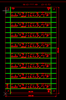
What is good panelization? There are two types. The first is the same PCB panelize in one sheet,see the right side.

To assemble quicker ,we will add four board edges with 10mm, and three fiducial (not four), and four tooling holes at the edges.
we will score the boards ,you can break them easily.
Same PCB panelization is easy,we just need to copy and paste .

If you panelization them by yourself,please note the board edges and space.
Please email to sales@stormcircuit.com , if you have any PCB questions.
​
Picture
Picture
Picture
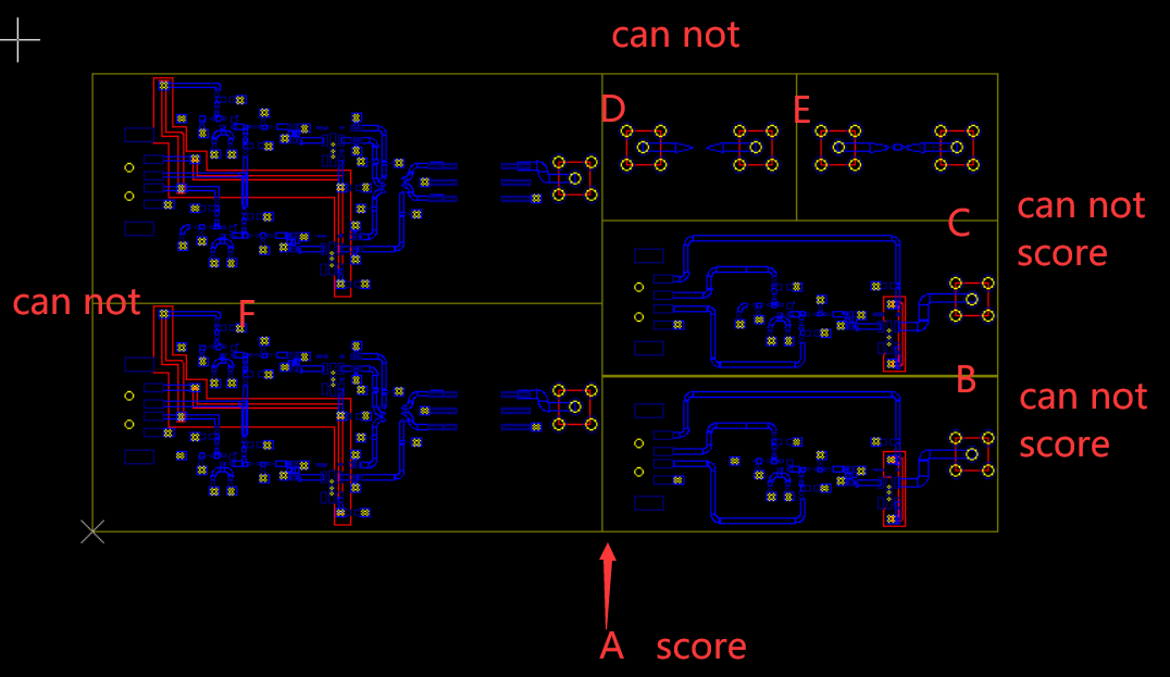
The second panelization type is the different PCB fit in one sheet.
​Many design customers would like to make some prototypes, and there are some different PCBs in one sheet. But a lot of the customers made wrong panelization. That makes our engineer hard to do .
see the left side.  There are three different designs ,two of each in the panel. But we can not make it as per the panel drawing.
We only can score (v-cut) the panel from A line,we can not score panels from the other lines .(B,C,D,E) it will damage another board when score. That makes you can not break them when you get the panel.
​Our engineers have to move the boards to get a space to rout or score.
This is the panel we have to change. we can make more boards to you ,but the score lines have to be ​ a vertical or horizontal straight line. or we will add 2mm space between each board.

Panelization tips

  1. The V-cut line should be the same as the outline of the Sub-PCB. That is to say, there is zero space between the sub-boards.
  2.  the score line can only be a vertical or horizontal straight line.
  3. The V-cut line must cross the whole panel or else the factory can't add a V-groove on the PCB because the milling cutter may destroy any sub-PCBs on the V-cut line. They also cannot stop part way across the panel. The V-cut lines shown below are not acceptable.
  4. The smallest panel size is 70*70mm, max can be 400*400mm, but we prefer under 300*300mm if possible, about A4 dimension (210*297mm) is the best size to do .
About Us
Why Us
WorkShop
Tips for PCB design
Testimonials
​Contact Us
Technology
Backdrilling PCB
Generate Gerber
Rigid-Flex Design Guide
10 Layer PCB
Impedance control
Heavy Copper PCB
​
PCB Assembly
Quick Turn Circuits
HDI boards
Rigid-Flex circuits
RF/Microwave/HF PCB
MC PCB/Al-substrate
ENEPIG PCB
​Components procument


order online
Payment
Shipment
FAQ
SMT stencil
Via in Pad (POFV)
0.38mm pitch CSP

Download
PCB Capability
Sample BOM
PCB check list
Multilayer stack up
​Stencils
PCB material

​
All rights reserved,2007-2022 Storm Circuit Technology  Ltd  
Blog: www.stormcircuit.net
Picture
storm pcb: www.stormpcb.com
Picture
Picture
Made with love  by Storm Circuit in China

Picture
Picture

    news and discount

Subscribe
  • Home
  • About Us
    • Why Us
    • Our Team
    • Testimonials
  • PCB Fab
    • Standard PCB
    • ENEPIG PCB
    • HDI PCB
    • Large PCB
    • Impedance Control
    • Backdrilling PCB
    • Heavy Copper PCB
    • Via in Pad(POFV)
    • Quick Turn PCB
    • 10 layer PCB
    • High frequency PCB
    • MC/Aluminum PCB
    • Half hole plating
    • FPC Rigid-flex PCB
  • Service
    • PCB Assembly >
      • PCBA Products
      • PCBA Capability
    • Components Procuement
    • SMT Stencil
  • Technology
    • Optimize HDI
    • PCB Terminology
    • PCB Material
    • PCB panelization
    • PCB Stackup
    • Rigid-flex PCB design guidelines
    • Blind and burrid vias
    • Tip for PCB design
    • Generate gerber from Altium
    • Eagle PCB
    • KiCAD PCB
  • Contact
  • Blog
  • Products