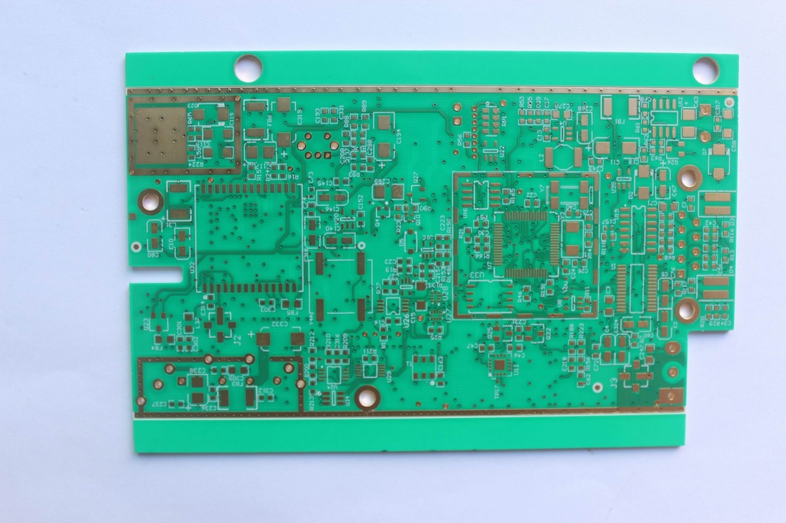
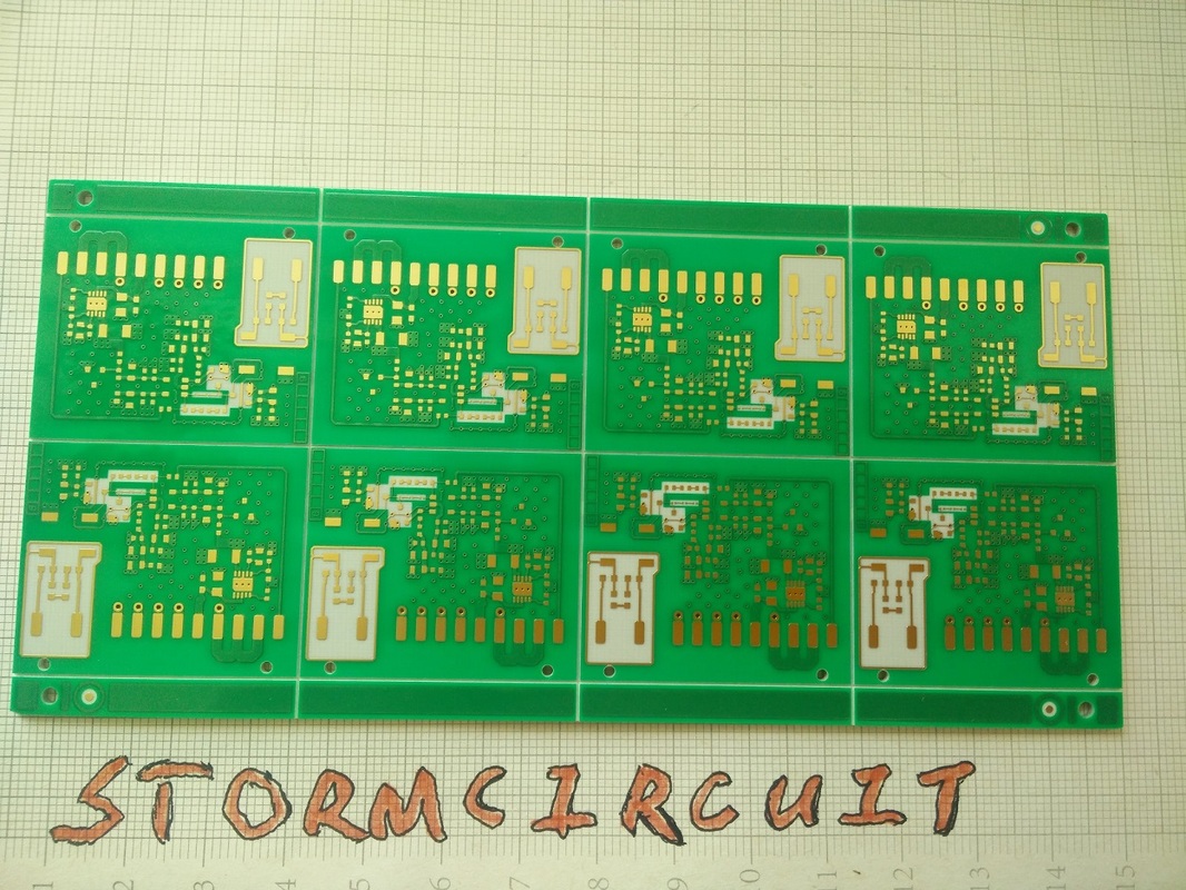
• Home
  • About Us
    • Why Us
    • Our Team
    • Testimonials
  • PCB Fab
    • Standard PCB
    • ENEPIG PCB
    • HDI PCB
    • Large PCB
    • Impedance Control
    • Backdrilling PCB
    • Heavy Copper PCB
    • Via in Pad(POFV)
    • Quick Turn PCB
    • 10 layer PCB
    • High frequency PCB
    • MC/Aluminum PCB
    • Half hole plating
    • FPC Rigid-flex PCB
  • Service
    • PCB Assembly >
      • PCBA Products
      • PCBA Capability
    • Components Procuement
    • SMT Stencil
  • Technology
    • Optimize HDI
    • PCB Terminology
    • PCB Material
    • PCB panelization
    • PCB Stackup
    • Rigid-flex PCB design guidelines
    • Blind and burrid vias
    • Tip for PCB design
    • Generate gerber from Altium
    • Eagle PCB
    • KiCAD PCB
  • Contact
  • Blog
  • Products
Quick Turn PCB ENEPIG PCB 10 layer PCB Turnkey Assembly Rigid-flex PCB
  • Home
  • About Us
    • Why Us
    • Our Team
    • Testimonials
  • PCB Fab
    • Standard PCB
    • ENEPIG PCB
    • HDI PCB
    • Large PCB
    • Impedance Control
    • Backdrilling PCB
    • Heavy Copper PCB
    • Via in Pad(POFV)
    • Quick Turn PCB
    • 10 layer PCB
    • High frequency PCB
    • MC/Aluminum PCB
    • Half hole plating
    • FPC Rigid-flex PCB
  • Service
    • PCB Assembly >
      • PCBA Products
      • PCBA Capability
    • Components Procuement
    • SMT Stencil
  • Technology
    • Optimize HDI
    • PCB Terminology
    • PCB Material
    • PCB panelization
    • PCB Stackup
    • Rigid-flex PCB design guidelines
    • Blind and burrid vias
    • Tip for PCB design
    • Generate gerber from Altium
    • Eagle PCB
    • KiCAD PCB
  • Contact
  • Blog
  • Products

High Frequency PCB

High frequency PCB also called HF PCB.The RF frequency range is typically from 500 MHz to 2 GHz, and designs above 100 MHz are considered RF. The microwave frequency range is anything above 2 GHz. There’s a considerable difference between RF and microwave circuits versus typical digital and analog circuits. In essence, RF signals are very high frequency analog signals. Therefore, unlike digital, at any point in time an RF signal can be at any voltage and current level between minimum and maximum limits. We have much experience in this filed,up to 60 GHz PCB we made.
  • Made of special Resin system material with Low ER and Low loss factor
  • Hybrid Build up mix of FR4 with Low loss material
  • Tight Impedance control
  • Used in Automotive, Radar, CAR to CAR communication, Distance Assistance, Active Drive Systems
We say high frequency ,also like RF PCB and microwave PCB as they are special material too,not usual FR4 .We have Taconic,Rogers,F4B,F4BM.PTFE material in stock.With this,we can do your special boards quick turn.Unlike other suppliers need long time to purchase material. 

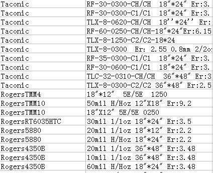
Here is an example for hybrid material stakcup. 
​RO 4003 8mil+FR4 TG170+RO4003 8mil.
Picture
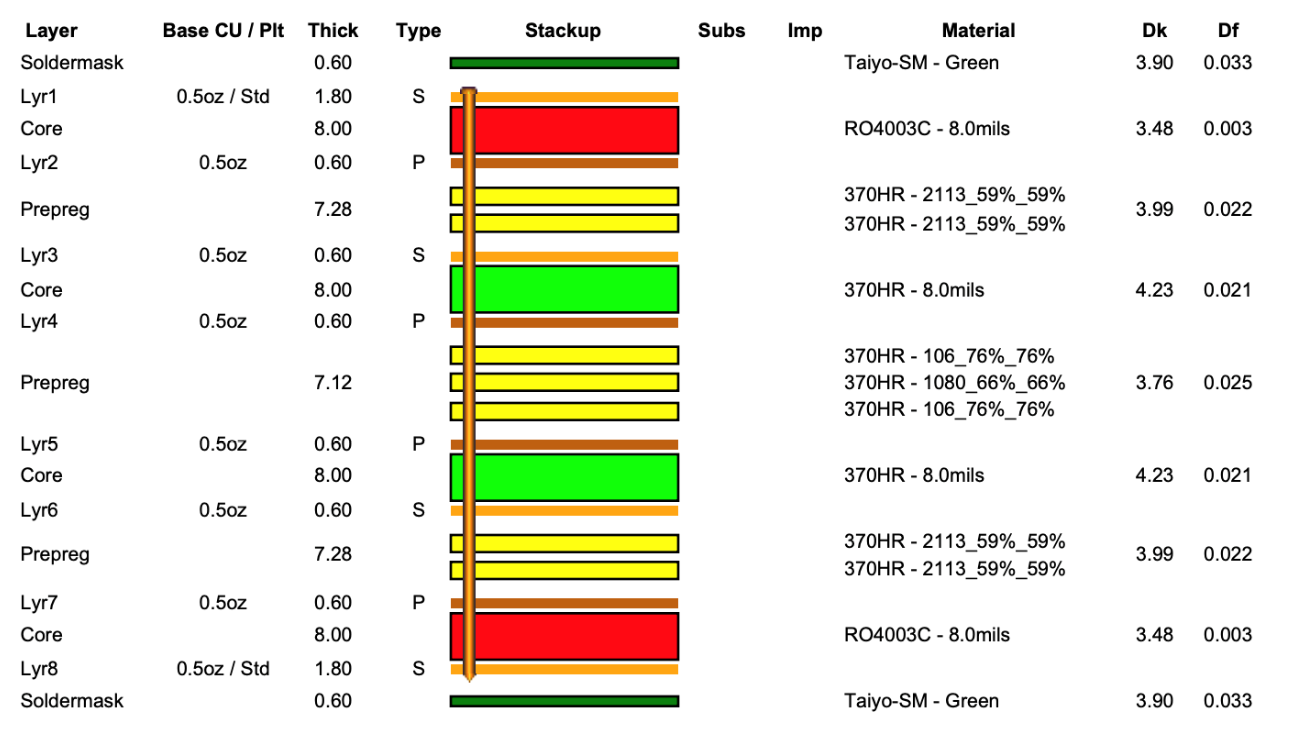
RO 4003 8mil+FR4 TG170+RO 4003 8mil
Get Your High Frequency PCB Quote Now
Taconic TLC-32(PTFE),Thickness=0.8mm,Er=3.2
Taconic TLC-32(PTFE),microwave
 Ceramic board for Panasonic ,thickness=1.0mm,High
frequency component moudle
 Ceramic board for Panasonic ,thickness=1.0mm,High frequency component moudle
6 layer RF board,Rogers 4350B+FR4,Hybrid stackup
6 layer RF PCB ,RO 4003C. Quick Turn 6 days.
6 LAYER RF PCB ,RO4003C
We have many High frequency material in stock .Here is just an example.Contact us to get more details.
Storm Circuit high frequency material in stock
2 layer RO 4350B 10 mil material ,quick turn 2 days.
Oregon State University.From Order to receive ,only 3 days.
RO 4350B PCB
Download

Mullilayer standard stack up
PCB Fab check list 
PCB capability
Sample BOM
Flex PCB material
High frequency material
Design guide for FPC
6 layer PCB with impedance control
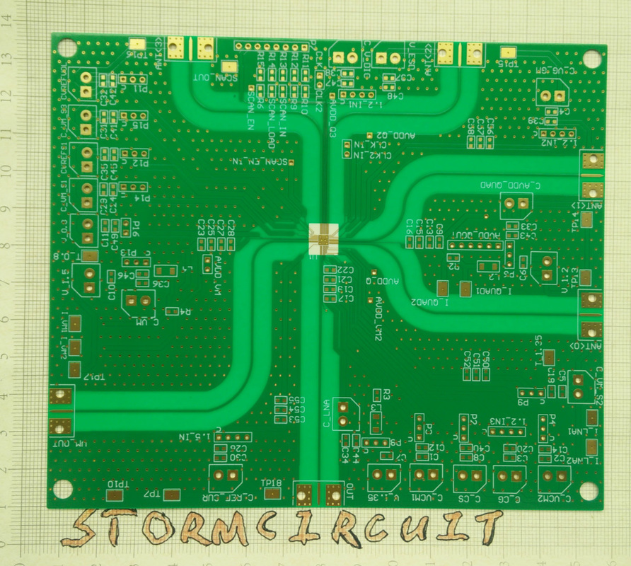
6 layer impedance control
Our PCBs

Flex PCB
Rigid-flex PCB
RF board
Heavy copper PCB
20 layer PCB
10 layer PCB
HDI PCB
ENEPIG PCB
Control impedance
Quick Turn boards
MC PCB
BOSCH boards with peel mask
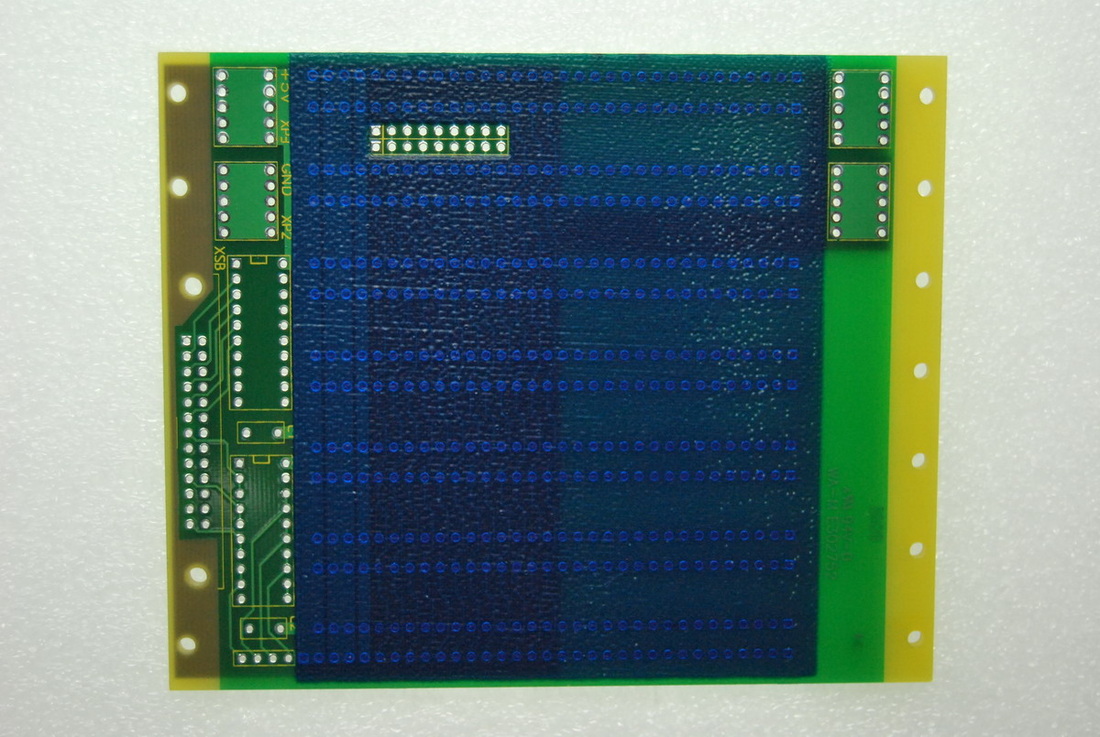
BOSCH boards with Peel mask
Additional Products&Service

Components Sourcing
PCB Assemble
SMT Stencil
Cable assemble

About Us
Why Us
WorkShop
Tips for PCB design
Testimonials
​Contact Us
Technology
Backdrilling PCB
Generate Gerber
Rigid-Flex Design Guide
10 Layer PCB
Impedance control
Heavy Copper PCB
​
PCB Assembly
Quick Turn Circuits
HDI boards
Rigid-Flex circuits
RF/Microwave/HF PCB
MC PCB/Al-substrate
ENEPIG PCB
​Components procument


order online
Payment
Shipment
FAQ
SMT stencil
Via in Pad (POFV)
0.38mm pitch CSP

Download
PCB Capability
Sample BOM
PCB check list
Multilayer stack up
​Stencils
PCB material

​
All rights reserved,2007-2022 Storm Circuit Technology  Ltd  
Blog: www.stormcircuit.net
Picture
storm pcb: www.stormpcb.com
Picture
Picture
Made with love  by Storm Circuit in China

Picture
Picture

    news and discount

Subscribe
  • Home
  • About Us
    • Why Us
    • Our Team
    • Testimonials
  • PCB Fab
    • Standard PCB
    • ENEPIG PCB
    • HDI PCB
    • Large PCB
    • Impedance Control
    • Backdrilling PCB
    • Heavy Copper PCB
    • Via in Pad(POFV)
    • Quick Turn PCB
    • 10 layer PCB
    • High frequency PCB
    • MC/Aluminum PCB
    • Half hole plating
    • FPC Rigid-flex PCB
  • Service
    • PCB Assembly >
      • PCBA Products
      • PCBA Capability
    • Components Procuement
    • SMT Stencil
  • Technology
    • Optimize HDI
    • PCB Terminology
    • PCB Material
    • PCB panelization
    • PCB Stackup
    • Rigid-flex PCB design guidelines
    • Blind and burrid vias
    • Tip for PCB design
    • Generate gerber from Altium
    • Eagle PCB
    • KiCAD PCB
  • Contact
  • Blog
  • Products